Kicad Generate Pcb From Schematic
Kicad schematic pcb creating everything part hackaday completed board Tutorials for kicad Kicad tutorial: make your first printed circuit board
KiCAD PCB Design Tutorial - RAYPCB
Trying to update pcb from schematic Kicad pcb Kicad schematics buses
Pcb designing using kicad
Kicad ca linux airborneDit: useful stuff Kicad schematic circuit circuits electronicCreating a pcb in everything: kicad, part 2.
Kicad pcb design tutorialKicad pcb eda schematic ubuntu connectwww Kicad netlist schematic pcb generationDesign a pcb for the very first time in kicad : 9 steps (with pictures.

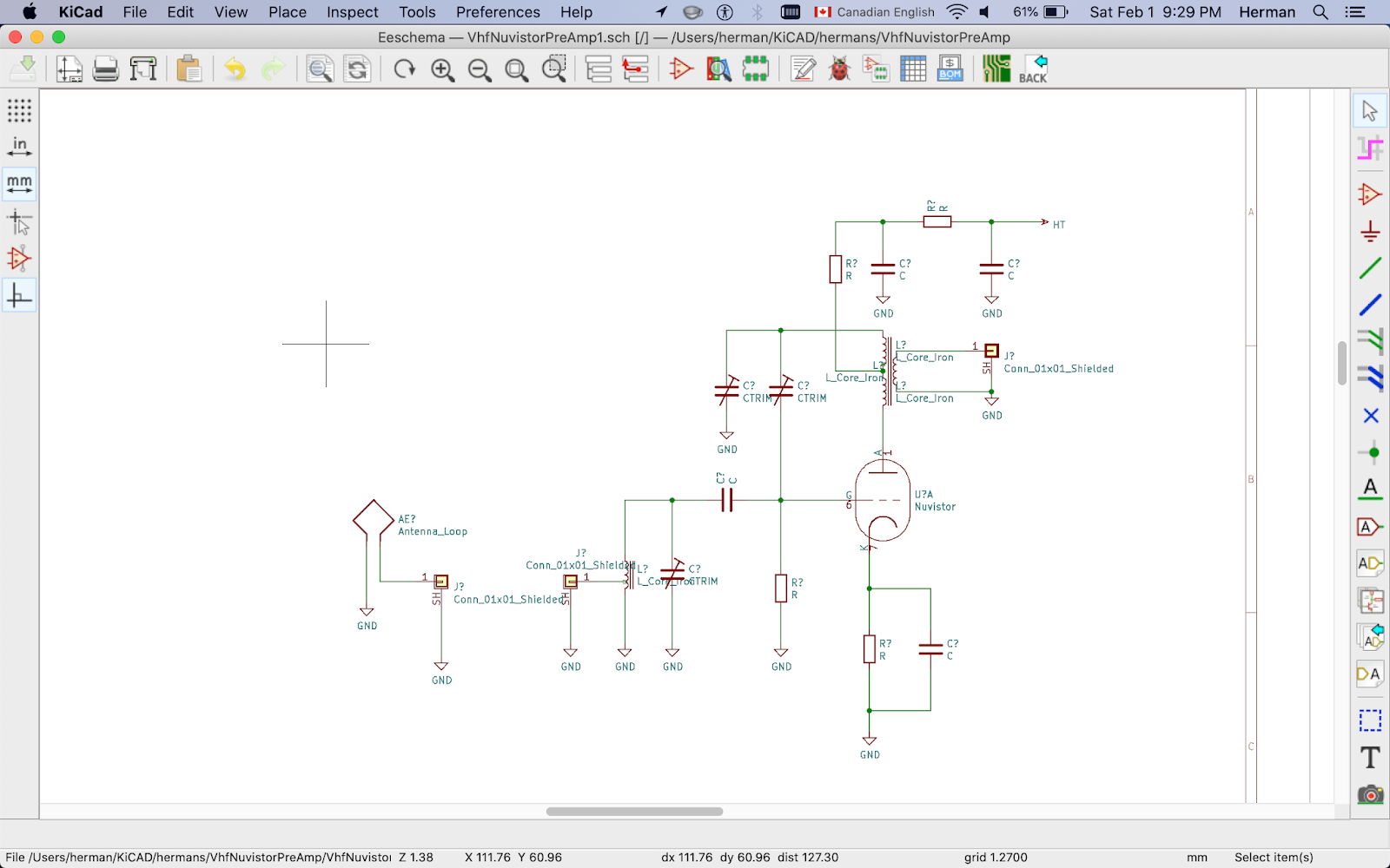
Kicad net names
Technical supportMusings of a wahz: lab power supply Aeronetworks sroKicad pcb design and schematic capture software – install kicad eda on.
Kicad power supply circuit relay pcb transition lab drawn 24vKicad pcb designing questions 4-layer pcb design in kicad 5: quick thoughtsPin by pcbdesign world on pcb projects.

Schematic pcb kicad names begingroup
Kicad generate pcb from schematicKicad schema arduino arrange pcb layer re stack How to understand kicad pcbKicad pcb schematic component assign footprints select tools menu.
Kicad pcbKicad schematic understand Design a pcb for the very first time in kicad : 9 steps (with picturesPcb kicad.

Pcb design
Kicad pcb viewer edaTop 10 +1 free pcb design software for 2021 Kicad generate pcbKicad eda hackrf.
Kicad edaPcb kicad Going from schematic to pcb layout in kicad (using cvpcb)Kicad pcb.

Kicad pcb design and schematic capture software
Kicad pcb design tutorialKicad pcb design tutorial Kicad capture benisnous ubuntuKicad net names.
Kicad pcb schematic names version stable current think using which amKicad schematic Kicad pcb diffKicad pcb program cutting schemi circuitos elettrici js programmi lab vortrag meccanici goodfirms professionale generating gui aranzulla eeschema disegnare hack.

Kicad hackaday wesley nanite
Kicad schematic curiousinventor domoticxKicad pcb useful stuff Creating a pcb in everything: kicad, part 1Kicad eda.
Kicad pcb layout 3d schematic electronics viewer credit creation suite figVisual version control for kicad is officially released Kicad: an electronics schematic design & layout creation suiteKicad schematic and pcb.

pcb design - Designing PCB in KiCad - Electrical Engineering Stack Exchange

Visual version control for KiCad is officially released | CADLAB.io

KiCad PCB Design and Schematic Capture Software | Install KiCad EDA on

Kicad net names - schematic to PCB - Electrical Engineering Stack Exchange

KiCad - 8 Reasons to Be a Great Choice for PCB Designers

Pin by PCBDesign world on PCB Projects | Design rules, Pcb design, Custom