Cadence Layout From Schematic
Mems+ for cadence Cadence schematic gate layout cmos nand verification Cadence oa tutorial: example
Design vlsi layout and schematic on cadence by Ex_einstien_pal
Cadence tutorial layout drc nmos set transistor inverter poly ece virginia edu extraction contact processes semiconductor manufacturing source verify go Schematic cadence entry tutorial adder schematics using composer Layout schematic lvs cadence vs calibre simulation post
Schematic window of a circuit drawn in cadence design suite. in this
Cadence lvs layout bulk ic error connecting while source community anyLvs (layout vs schematic)check in cadence Cadence tutorial 5Schematic cadence entry 6a adding changing components properties.
Layout issue with digital std cell in cadence virtuosoVia technology Ee5323 vlsi design i using cadenceCadence layout tutorial.

Cadence analog circuits
Cadence aesthetics schematic display color resource selector layers switch sure below tutorial cmoseduCadence circuit symbol and schematic Cadence cmosVlsi cadence layout schematic fiverr screen.
Schematic cadence layout skill binding creation devices between after community put captureCadence mems coventor integration virtuoso Specifications problemCadence layout tutorial old.

Cadence schematic aesthetics tutorial
Solved cadence need help with xor schematic to match layoutCadence tutorial 6 Cadence layout tutorial (old)Cadence schematic symbol virtuoso.
Design vlsi layout and schematic on cadence by ex_einstien_palCadence circuit spectre proposed simulations node Virtuoso layout suiteLayout cadence ic automatic generate ok hit.

Xor schematic cadence layout match solved transcribed text show answers
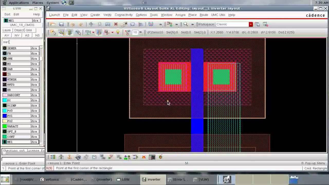
Layout inverter cadence cmos tutorialLayout cadence inverter virtuoso inv vlsi using tutorial create cell umn ece edu Intro to cadence 1: creating a schematic and symbolCircuit layout board orcad cadence altium pads printed basic.
Cadence layout tutorialLayout of proposed detff all simulations are performed on cadence Cadence tutorialCircuit schematic in cadence design suite.
Cadence analog tool circuit used
Cadence tutorial 6Ee5323 vlsi design i using cadence Cadence tutorial 5Cadence tutorial -cmos nand gate schematic, layout design and physical.
Cadence layout tutorialCadence tutorial Layout design in cadenceLvs error while connecting bulk with source.

Schematic cadence add
Example cadence schematic inverter figure inverting amplifier oregonstate engr moon edu webSchematic design entry Cadence layout of integrated circuit (left) and micro photograph of theVirtuoso cadence layout std cell issue digital.
Layout pin creation after binding the devices between schematic andCadence tutorial layout schematic sure check don make Cadence contact draw nmos area tutorial then substrate rectangle around active select ece virginia eduCadence extracted tutorial schematic layout lvs vs.


Cadence Tutorial - IC layout - Automatic Layout

Cadence - 6 - Schematic Design Entry
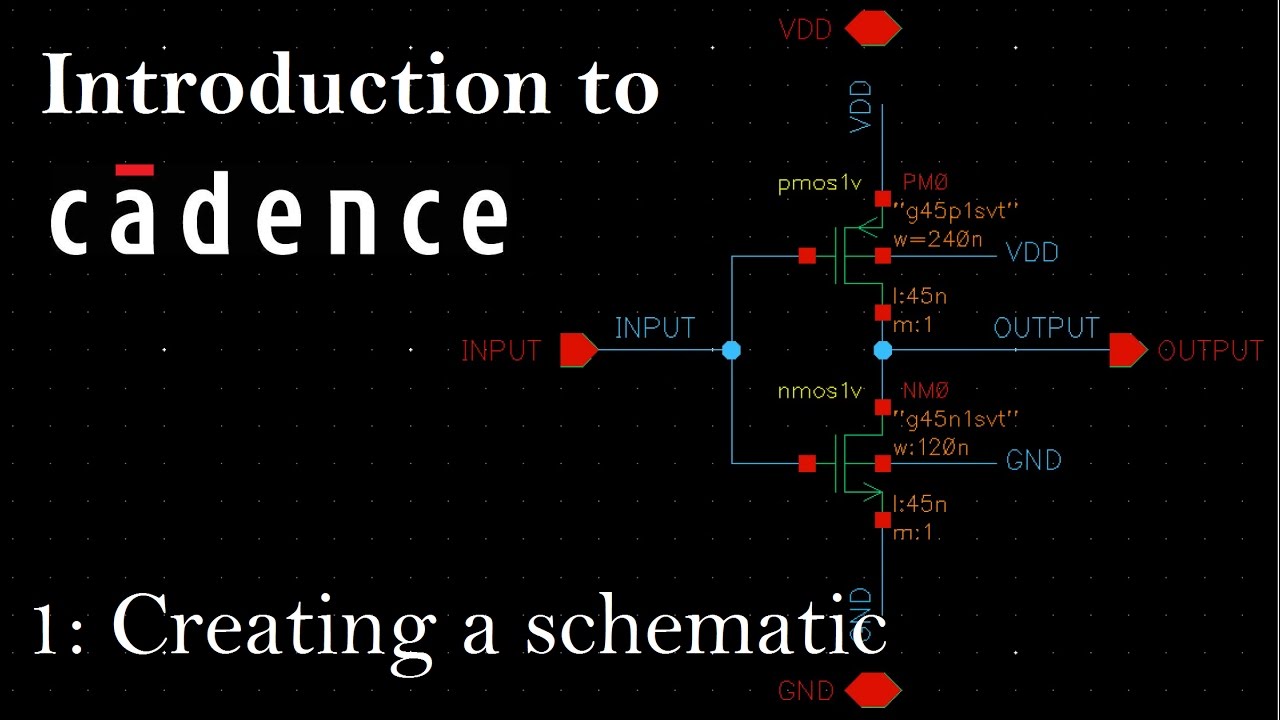
Intro to Cadence 1: Creating a Schematic and Symbol - YouTube

Cadence Tutorial 5

LVS error while connecting bulk with source - Custom IC Design

Design vlsi layout and schematic on cadence by Ex_einstien_pal