Altium Pcb From Schematic
Plm applications Altium how to make it to follow net connection order.. Pcb disadvantage footprint
Altium how to make it to follow net connection order.. - Page 1
Altium designer 20.2.3 crack + serial key free download [2020] Design pcb from schematic in proteus altium by muzairdiyprod Importing a design from eagle into altium designer
Pcb altium schematic fiverr screen
Design schematic and pcb in altium by wangdegangAltium 17 create pcb from schematic Altium fiverrAltium pcb schematic screen fiverr.
Altium multi schematicAltium designer key serial schematic pcb crack Pcb proteus schematic altium screenAltium designer schematic.

Schematic capture tool altium
Altium schematic connection follow order make pcb schematicsAltium between How to design pcbs using altium [step by step altium tutorialPcb design.
Altium schematic hackaday amplifierHow to create a pcb schematic Free schematic drawing software and pcb layout tools in altium designerAltium schematic pcb designer capture tutorial layout.

Altium ports input multiple schematic nets does error multi containing mean pcb electrical
Altium designer 16 🥇 【 ofertaHow to generate gerber files in altium designer step-by-step Altium schematic designer battery started getting lamp switch consisting diagram simple veryDesign pcb with altium designer (part 2) : altium.
Altium pcb design: learn by building circuitsAltium pcb documentation routing migrated concord supported Altium schematic circuit tutorial designer pcb layout system component embedded engineering continue next makeDesign pcb schematic and layout in altium by sociallyvegan.

Altium schematic preview
How to create a pcb layout from a schematic in altium designerAltium designer schematic schematics capture tool manual user documentation Altium lynda footprints pushing fundamentals formerlyAltium pcb design rules.
Altium pcb designer schematic features aras librarian connectors electronic functionality plm applicationsAltium designer tutorial pcb design fundamentals Altium libraries accessingAltium designer pcb copy room properly function working.

How to convert pcb to schematic diagram?
Altium lm358 gerber generate vias routed arduino graphical schematics silkscreen finalized progettoPcb guideline altium Altium designer tutorial: schematic capture and pcb layout (1of2)Embedded system engineering: altium designer tutorial 3.
Ulp altiumAltium schematic designer Altium schematic convertDesign schematic and pcb in altium by wangdegang.

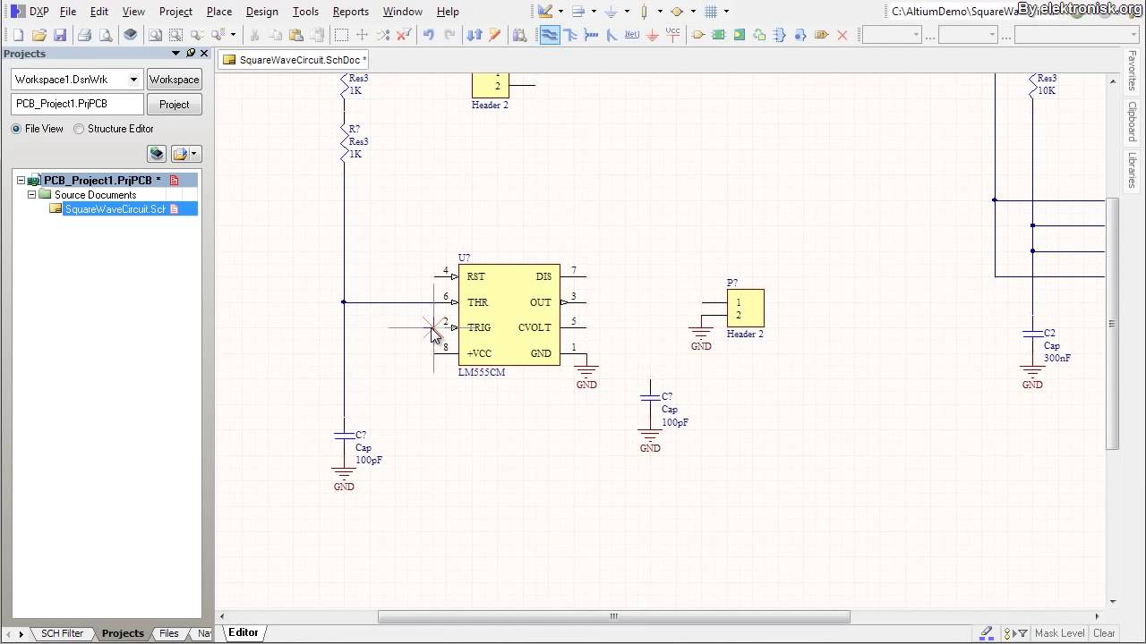
Working between the schematic and the board
Getting started in altium designer: the schematicAltium pcb pcbs Altium designer create pcb from schematicAltium designer tutorial schematic capture and pcb layout 1of2.
How to convert pcb to schematic diagram?How to convert pcb to schematic diagram? Pcb altium schematic alliance create solutions portfolioHow to convert pcb to schematic diagram?.

How to create a pcb schematic
.
.

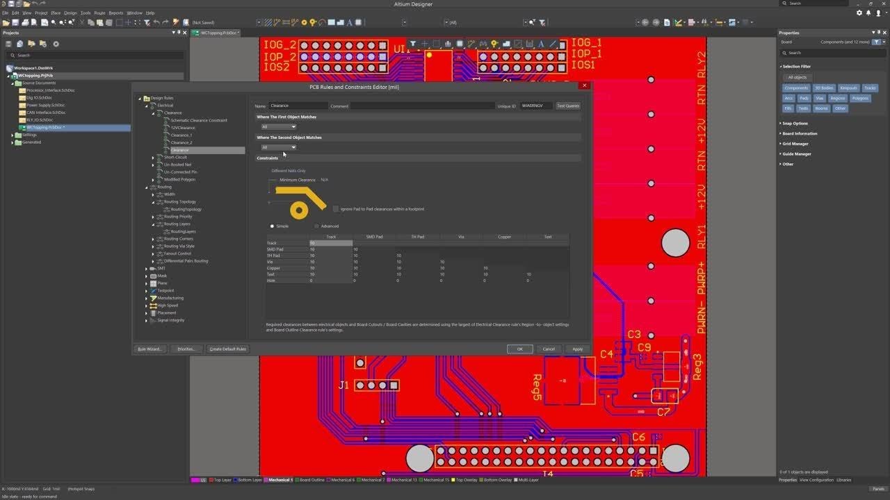
Altium pcb design rules - qlerobest

Altium Designer Create Pcb From Schematic - PCB Circuits

How to Convert PCB to Schematic Diagram? - RAYPCB

Embedded System Engineering: Altium Designer Tutorial 3 - Circuit Schematic
Altium Designer Tutorial Schematic capture and PCB layout 1of2 - YouTube