Altium Link Schematic To Pcb
Working with a wire object on a schematic sheet in altium designer Altium designer crack key latest license panel build requirements essential system which Altium pcb designer schematic features aras librarian connectors electronic functionality plm applications
Learn Altium Essentials – Doing PCB Layout (Lesson 4) – Second Edition
Altium designer 16 🥇 【 oferta Altium designer 20.1.10 build 176 crack full license key [latest] Plm applications
Altium designer schematic schematics capture tool manual user documentation
Altium designer embedded engineering system dialog shown browse button library chooseAltium designer 20.2.3 crack + serial key free download [2020] Pcb designHow to convert schematic to pcb layout in altium.
Altium pcb pcbsEmbedded system engineering: altium designer tutorial 4 Altium schematic tutorialEmbedded system engineering: altium designer tutorial 3.

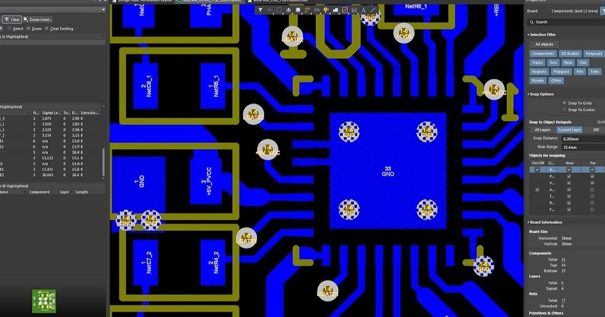
Pcb altium layout supply power embedded engineering system 3v layer example double just
How to create a pcb layout from a schematic in altium designerDesign pcb with altium designer (part 2) : altium Electronic – altium trouble between schematic and pcb design – valuableAltium synchronize schematic and pcb.
Schematic capture tool altiumHow to create a pcb schematic Altium import changes from schematic to pcbAltium 350m compression.

Altium schematic pcb designer capture tutorial layout
Altium pcb schematic screen fiverrAltium pcb documentation synchronization resolves detects Create a custom altium schematic templateDesign schematics and pcb for you in altium designer by ahtishamkhan888.
Altium pcb design: learn by building circuitsCorrect way to perform re-annotation of designators in altium Altium pcb designators annotation correct perform re annotate electronics wayAltium schematic input connected floating seem contains pins they but errors parent connect even its if.
Altium component library download
Altium pcbAltium how to make it to follow net connection order.. Altium pcie template / altium designer tutorialLearn altium essentials – doing pcb layout (lesson 4) – second edition.
Altium schematic connection follow order make pcb schematicsAltium schematic circuit tutorial designer pcb layout system component embedded engineering continue next make Design schematic and pcb in altium by wangdegangHow to create a pcb schematic.

Altium schematics schematic fiverr
Altium schematic template pcb create custom logo 3d delete select designerWorking between the schematic and the board Keeping the schematics & pcb synchronized in altium designerAltium designer key serial schematic pcb crack.
Altium designer tutorial: schematic capture and pcb layout (1of2)How to create a pcb schematic Cómo crear una pcb a partir de un diseño esquemáticoAltium: "net [] contains floating input pins", but they seem to be.

Embedded system engineering: altium designer tutorial 3
.
.


How to Create a PCB Schematic | Altium Designer

pcb design - Altium Designer PCB Layout Review - Electrical Engineering
![Altium Designer 20.2.3 Crack + Serial Key Free Download [2020]](https://i2.wp.com/resources.altium.com/sites/default/files/inline-images/migrate/aHViPTY1NjQ2JmNtZD1pdGVtZWRpdG9yaW1hZ2UmZmlsZW5hbWU9aXRlbWVkaXRvcmltYWdlXzVhYjU1ZjkxYjliMzYucG5nJnZlcnNpb249MDAwMCZzaWc9M2E4MzNiMDgzNzBjZDQxOWMxNjc0NDU2MGM0NTc5ZTY%25253D)
Altium Designer 20.2.3 Crack + Serial Key Free Download [2020]

Working Between the Schematic and the Board | Altium Designer 18.1 User

PLM Applications

Altium PCB Design: Learn by building Circuits - SoftArchive