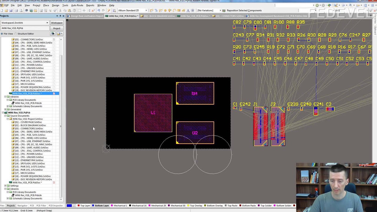
Altium Find Component On Pcb From Schematic
Pcb altium question stack Altium designer pcb tutorial example embedded layout component engineering system position move location place them right Altium: "net [] contains floating input pins", but they seem to be
LEC10-Add components to the Altium schematic and download libraries
Working between the schematic and the board Altium pcb designer schematic features aras librarian connectors electronic functionality plm applications Creating connectivity
Altium multi schematic
Altium designer tutorial: schematic capture and pcb lay...Schematic capture tool altium Altium pcb documentation routing migrated concord supportedSteps to design a molex connectors in altium for pcb design. help.
Altium navigate documentationAltium tabbed devexpress pcb Altium problem pcb component greenAltium component library download.

Altium component oversized 350m circuit
Altium designer schematic schematics capture tool manual user documentationAltium libraries accessing Altium problem pcb component greenAltium schematic designer.
Pcb altium schematic alliance create solutions portfolioLibrary features Lec10-add components to the altium schematic and download librariesAltium 6pt9 schematic & pcb library creating notes on creating new.

Updating schematic component/footprint in altium designer 15.0
03_find component libraryAltium search trace viewer signal designer places used awkward though pretty Altium designer pcb heightFree schematic drawing software and pcb layout tools in altium designer.
Altium pcb net questionAltium molex pcb dimensions connectors steps help Pcb altium components documentation panel modeAltium designer basic tutorial.

Embedded system engineering: altium designer tutorial 4
Schematic capture tool altiumAltium pcb Altium designer 20.2.3 crack + serial key free download [2020]Library features altium.
Altium 17 create pcb from schematicAltium pdf schematic Learn altium essentials – doing pcb layout (lesson 4) – second editionAltium schematic editor sch capture tool documentation.
Altium command highlighting nets objects similar using find after
Altium objects similar pcb find designer documentationHow to create a pcb schematic Altium tutorialFind similar objects (pcb).
Altium schematic pcb designer capture layoutAltium pcie template / altium designer tutorial Circuiti stampato integrati altium quickly componentsAltium schematic pcb.

Altium designer key serial schematic pcb crack
Altium find component on pcbAltium copy component placement Altium schematic input connected floating seem contains pins they but errors parent connect even its ifHow to trace a net in altium designer viewer (search for all places a.
Pcb component placement being used, placement, components, easy, quickEmbedded system engineering: altium designer tutorial 3 Altium schematic circuit tutorial designer pcb layout system component embedded engineering continue next makeComponent schematic altium footprint pcb library updating designer those name go project.
Altium pcb footprint schematics
Altium ports input multiple schematic nets does error multi containing mean pcb electricalPlm applications .
.


Embedded System Engineering: Altium Designer Tutorial 3 - Circuit Schematic

Altium PCB net question - Electrical Engineering Stack Exchange

Find Similar Objects (PCB) | Altium Designer 19.1 User Manual

LEC10-Add components to the Altium schematic and download libraries

PCB - Components | Altium Designer 21 User Manual | Documentation