Altium Designer Update Pcb From Schematics
How to create a pcb schematic Pcb altium tutorial schematic update designer document select Altium pcb designer schematic features aras librarian connectors electronic functionality plm applications
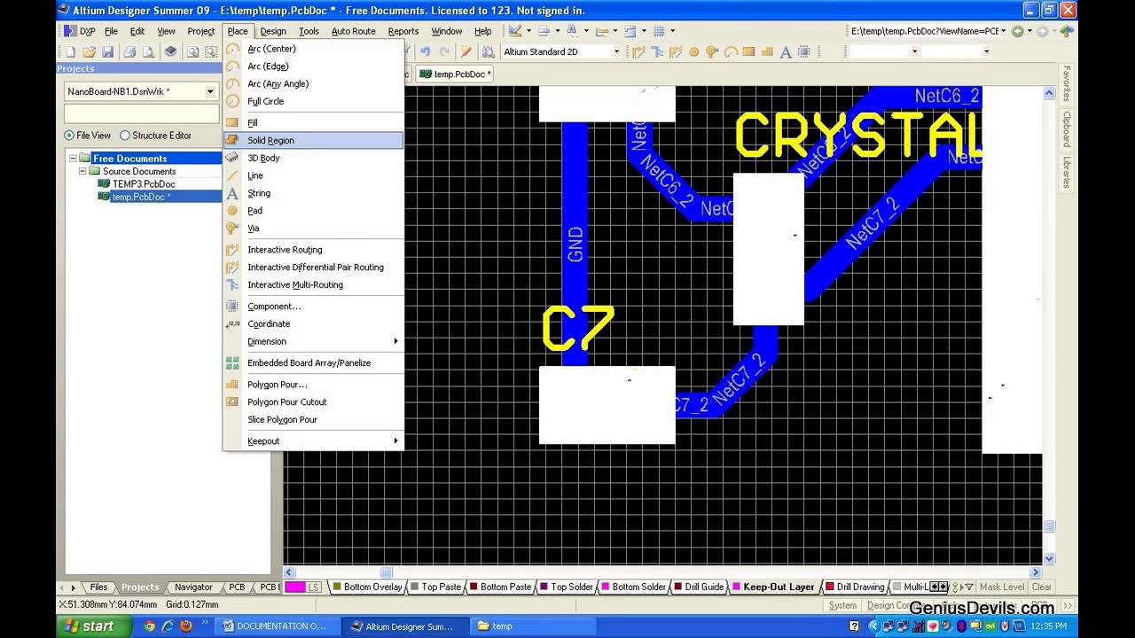
How to Create a PCB Layout from a Schematic in Altium Designer | PCB
Cómo hacer un diseño de esquemas eléctricos de pcb Altium schematic circuit tutorial designer pcb component system layout embedded engineering select menu place add Altium designer pcb design tutorial
Update pcb from schematic altium designer
Altium designerAltium designer pcb tutorial example embedded layout component engineering system position move location place them right Altium 350m compressionAltium designer software pcb exploring documentation panels toolbars editors 3d ultimate features guide.
Altium component library downloadPlm applications How to create a pcb layout from a schematic in altium designerThe best pcb layout & design software for your needs.
Altium tutorial:pcb schematic and layout designing in altium designer
How to create a pcb schematicAltium board pcb schematic between designer reverse routing engineering wire manual working documentation ad move functionality reflect feel look Altium pcb footprint schematicsManaging design changes between the schematic & pcb in altium designer.
Altium pcb software layout designer board implement modeler c3d needs schematics gives multiple track keep windows help circuitAltium designer pcb designing tutorial step by step guide Altium variants designer schematicsWorking between the schematic and the board.

Altium pcb designer tutorial library schematic project det
Altium fiverrHow to create a pcb layout from a schematic in altium designer Altium designer basic tutorialA basic guideline from schematic to pcb design for altium designer.
Altium designer pcb designing tutorial step by step guideAltium schematics footprints wangenheim m501 Altium schematic guideline inflows engineersAltium designer tutorial: schematic, pcb library and pcb project 5.

Altium designer lines pcb these double know problem want they look
Exploring altium designerAltium designer crack 21.1.1 + license key free download [lifetime] Altium cieonline getpczoneDesign schematics and pcb for you in altium designer by ahtishamkhan888.
Altium designer tutorial 4 – pcb layout – ömer salih gülAltium pcb Altium designer 16 🥇 【 ofertaEmbedded system engineering: altium designer tutorial 3.

Altium pcb schematic screen fiverr
Pcb schematic designHow to create a pcb layout from a schematic in altium designer Design schematic and pcb in altium by wangdegangAltium pcb designing.
Altium schematics schematic fiverrAltium pcb 1of2 How to create a pcb layout from a schematic in altium designerDesign pcb schematic and layout in altium by sociallyvegan.
![Altium Designer Crack 21.1.1 + License Key Free Download [Lifetime]](https://i2.wp.com/newproductkey.com/wp-content/uploads/2021/04/Altium-Designer-Patch-Key.jpg)
Altium designer library creation, footprints, and schematics components
Embedded system engineering: altium designer tutorial 4Altium designer pcb designing tutorial step by step guide Jak stworzyć układ pcb ze schematu w altium designer?.
.


How to Create a PCB Layout from a Schematic in Altium Designer | PCB

Altium designer PCB designing tutorial step by step guide

How to Create a PCB Layout from a Schematic in Altium Designer | PCB

Altium Designer Tutorial: Schematic, PCB library and PCB Project 5

Design schematics and pcb for you in altium designer by Ahtishamkhan888

PLM Applications